Senior Principal Scientist - InP Lasers (industrial PIC's)
- Hybrid
- Eindhoven, Noord-Brabant, Netherlands
- Technical Competence Centre TCC
Because this is one of the very few places where the transition from InP research to real 6-inch industrial production is still open, visible, and not yet decided.
Job description
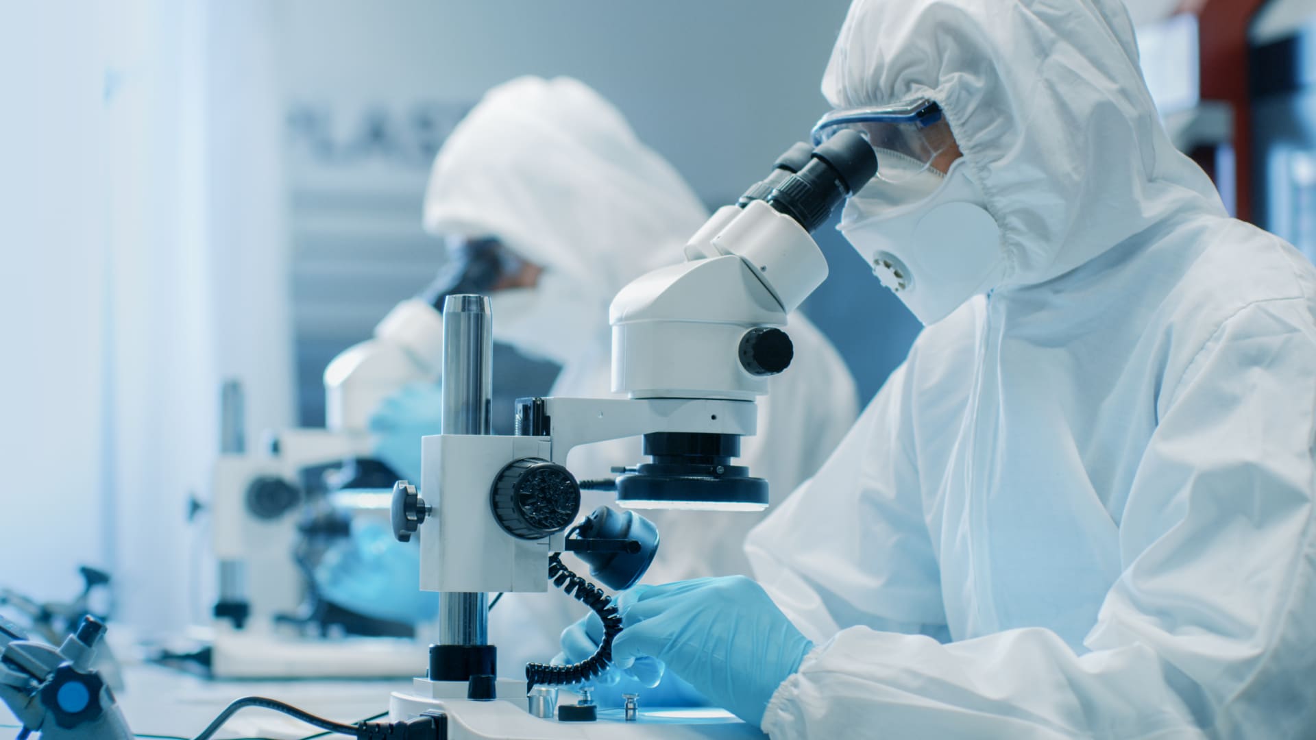
Why SMART Photonics
Because this is one of the very few places where the transition from InP research to real 6-inch industrial production is still open, visible, and not yet decided. Your technical judgement directly shapes how that gap gets closed.
You won’t just improve a device; you will be part of defining how Europe actually builds a photonic industry.
What you will do
Define where our InP laser platform goes next, including DFB and beyond.
Decide which ideas are worth scaling and which are not
Push concepts through to something that survives production; Work directly operations, R&D, test, and customers
You will be visible externally through conferences and invited talks, participation in technology consortia and collaborations, direct interaction with key customers, and representation at industry and sales exhibitions.
You are expected to bring your own ideas, challenge current approaches, start things that do not exist yet, and carry responsibility for whether they hold up in reality.
What you bring
Someone who has already brought photonic devices into real production
You understands yield, variability, and failure modes in practical.
You are comfortable making decisions with incomplete data and have enough credibility to challenge both engineers and leadership
You have seen where theory breaks and know how to respond when it does.
Job requirements
Essential Requirements;
Ph.D. in Photonics. and 15+ years of industrial experience in semiconductor photonics, with a strong focus on InP PICs.
Demonstrated, hands-on expertise in datacom laser technologies, including DFB lasers, at wafer scale.
Proven experience bringing photonic devices from R&D into stable, manufacturable production.
Available for an onsite position at the High Tech Campus in Eindhoven (NL), Working in a hybrid construction is possible.
Willingness to travel for conferences, customer visits, and collaborations. (15%)
Strong sense of ownership and long-term responsibility for technology decisions.
Technical Depth
You should be deeply comfortable with:
InP epitaxy–device–process interactions
Laser physics, cavity design, and mode control
Electrical and thermal effects in integrated lasers
Wafer-level variability, yield, and reliability considerations
Industrial fab environments and foundry constraints
You know where theory ends and where reality begins.
Leadership & Influence
Recognized as a technical authority by peers, customers, or the broader photonics community.
Able to influence without hierarchy, using clarity, credibility, and data.
Comfortable challenging assumptions; including your own.
or
All done!
Your application has been successfully submitted!
You've already applied for this job
We appreciate your interest in this position. Unfortunately, you have already applied for this job.