Senior Mask Design Engineer- Automation
- On-site
- Eindhoven, Noord-Brabant, Netherlands
- Design
You don't build infrastructure for the team, you build it with the team
Job description
We are looking for a Senior Mask Design Engineer with deep technical expertise to operate at the interface of technology and customer needs.
Meet the Team
Our Design Enablement team bridges process development, device design, and PIC circuit designers. We provide the tools, methodologies, and services that enable our customers to translate their concepts into manufacturable PICs.
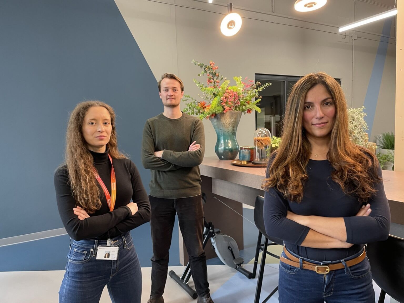
You will work in a team of 10 motivated and eager Engineers, and report to the Cluster Lead and Principal Scientist.
Purpose of the Role
Execute and improve the end-to-end tape-out flow for SMART Photonics' photonic integrated circuit platforms.
Your main role is to run tape-outs, understand the full post-processing chain, and own your deliverables. But there’s a special task that differentiates the one of a Mask Design Engineer! You will be responsible to automate, modularize, and harden the scripts and workflows you and your colleagues use every day.
You don't build infrastructure for the team, you build it with the team, raising the automation capability of the entire mask engineering group while keeping your own hands in the tape-out work.
Key Responsibilities
Tape-Out Execution
Perform full tape-outs: super-cell creation, PCM cell generation, layer post-processing, GDS validation, and mask ordering
Prepare and validate GDS files for mask production
Conduct Design Rule Checks (DRC) and ensure compliance with manufacturing rules.
Post-Processing Script Development
Develop, refactor, and maintain the Python and ruby based scripts
Make scripts that are modular, reusable, and platform-independent
Build supporting tooling for the tape out flow or users of our mask sets
Automation & Infrastructure Improvement
Identify repetitive, error-prone, or manual steps in the tape-out flow and automate them
Set up and maintain CI validation for post-processing outputs (regression against platform reference files)
Establish reproducible development environments for tape-out scripting
Introduce automated checks for steps that currently rely on manual verification
Contribute to repository structure, naming conventions, and Git workflow standards
Ensure every automated solution is understood, documented, and maintainable by the team, not just by you
Collaboration & Reporting
Review code from colleagues (quality, correctness, maintainability)
Collaborate with process integration, R&D, metrology, and procurement different projects
Coordinate with EDA, PDK and IT engineers on environment, tooling, and access topics
Job requirements
MSc or PhD in Electrical Engineering, Applied Physics, Photonics, or a related field’
7 + years (post-master's) OR 5 + years (post-PhD) of experience in a photonics foundry, PIC design house, EDA provider or customer-facing design enablement role.
Strong communicator, confident, and able to influence, build trust, and support leadership when needed.
Proactive learner who embraces new methods, tools, and industry best practices.
Leadership potential: able to own projects independently, drive departmental initiatives, and mentor colleagues.
High quality mindset with attention to details.
Proficiency in Python and/or Ruby
Working knowledge of Git and version control workflows
Familiarity with GDS-II file format and layout tools (KLayout, Nazca, or similar)
A natural tendency to automate repetitive work, the kind of person who runs a manual process twice and then scripts it
Preferred Qualifications
Experience in a semiconductor or photonic foundry environment
Understanding of DRC concepts and layer-based processing
Exposure to EDA tools (Synopsys OptoDesigner, Ansys Lumerical, or similar)
Experience with CI/CD pipelines
Tools & Technologies
Python, KLayout, Gitea/Git, GDS-II, CI/CD pipelines, Nazca
We offer:
Competitive salary, to be aligned with Recruiter on the first interview.
A challenging and impactful role within a fast‑growing high‑tech environment.
State‑of‑the‑art photonic technologies and advanced modelling tools.
A highly passionate, international team of experts in photonics and semiconductor technology.
Tailored learning and development opportunities: training, coaching, and on‑the‑job growth.
or
All done!
Your application has been successfully submitted!
You've already applied for this job
We appreciate your interest in this position. Unfortunately, you have already applied for this job.