(Senior) Device Integration Engineer
- On-site
- Eindhoven, Noord-Brabant, Netherlands
- integration engineering
Ensure seamless integration across the full value chain!
Job description
Introduction
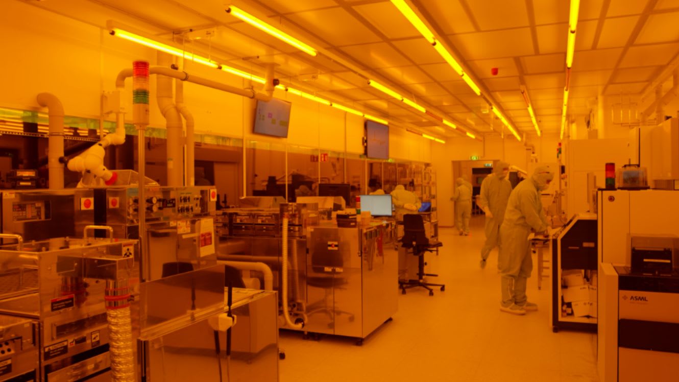
SMART Photonics B.V. is a pure-play Indium Phosphide (InP) photonic foundry. We work closely with customers across telecom, datacom, sensing, and quantum to turn innovative ideas into high-performance photonic integrated circuits (PICs).
Why this role exists:
As an InP foundry, SMART's strength is in frontend processing and device design. Our chips, however, must succeed inside packages built and qualified by our customers and partners. As product complexity and volumes grow we would like to enhance this connection between our frontend choices and the packaging realities: translating packaging requirements into design rules, assessing compatibility of our process modules with industry-standard packaging techniques, and ensuring our PICs are packaging-ready by construction. This will be the focus of this new senior individual contributor role within our Product & Integration Engineering (PIE) team.
The team you'll work with:
You'll join a strong and diverse PIE team!
Three Device Integration Engineers focused on EOL PCM, EOL data analysis, and understanding device-level design enablement; four Vertical Integration Engineers focused on process flow, in-line PCM, and issue resolution; and a dedicated statistician supporting data analysis across the value chain. You'll partner closely with our Design Enablement team, Test & Measurement Reliability team, Backend team as well as external partners for backend, packaging, and testing.
This is a role where collaboration skills are crucial for long-term success.
What you'll do:
Own the bridge between our frontend and packaging.
Establish and maintain Design-for-Packaging rules and process specifications that connect our InP foundry capabilities to the packaging techniques our customers and partners use. Translate learnings into PDK updates, in close collaboration with the Design Enablement team.
Assess process-to-packaging compatibility.
Evaluate whether our bondpads, planarization, metallization stacks, layout patterns, and other process modules are compatible with die attach, wire bonding, fiber alignment, and assembly methods used in the industry. Identify gaps and drive corrective actions through design or process changes.
Lead packaging-integration aspects of flagship programs.
We have several customer-partnership program, both at the advance stages where the focus is optimization and packaging compatibility for chips that are already processed and characterized as well as new platforms with the opportunity to influence designs for packaging readiness from an early stage. Examples are integrated iTLA and DFB demo programs.
Ensure that frontend-to-packaging decisions account for backend and reliability realities.
Coordinate with our Backend team (internal and outsourced via our future OSAT partner) on backend process implications, and with the T&M Reliability team on reliability outcomes. Evaluate supplier and partner results on pull and shear tests, qualification reports, design rule conformance, bring physics-aware interpretation to reliability data – all to make sure that both backend and reliability are well accounted in questions of packaging.
Drive yield improvement
By connecting packaging and reliability outcomes with in-line and EOL data across the value chain.
Lead cross-functional integration projects
Ensuring clear technical direction, alignment with stakeholders, and timely delivery.
Job requirements
Want to join the team? These are the skills we are looking for!
Essential:
Master's or PhD in Integrated Photonics, Electrical Engineering, Materials Science, Physics, or a related field.
Strong experience in photonic or optoelectronic semiconductor process integration or device design, with a strong understanding of how frontend choices propagate into packaging readiness.
Demonstrated experience establishing or contributing to Design-for-Packaging (or related DfX) rules, ideally translated into PDK and process specification.
Strong cross-functional communication. This role exerts influence rather than direct authority; we need a senior engineer whom other senior engineers will trust.
Familiarity with PIC design tools such as KLayout, Nazca, Luceda, or similar.
Highly valued:
Demonstrated experience in aligning packaging suppliers with device design and processing for PICs.
Hands-on experience with photonic or optoelectronic packaging techniques: die attach, wire bonding, optical fiber alignment and attach, hermetic and non-hermetic assembly.
Experience with InP-based photonics (lasers, modulators, integrated devices).
Ability to interpret reliability data (HTOL, damp heat, thermal cycling, and similar) in the context of underlying device physics.
Hands-on experience with photonic device characterization at die and packaging level;
Experience evaluating supplier or OSAT qualification data.
What we offer
A collaborative atmosphere with talented, passionate colleagues within an open culture.
Personalized career development, including training and coaching opportunities. Notable trainings: JePPIX courses, Green/Black Belt in DfSS and Six Sigma, and Project Management certifications.
For candidates who need a work permit, visa, and/or relocation, we are eligible to apply for the Dutch highly skilled migrant visa, and we have a relocation package in place.
Unique office perks such as chair massages, fresh fruit, fitness discounts, and Lunch Walks
or
All done!
Your application has been successfully submitted!
You've already applied for this job
We appreciate your interest in this position. Unfortunately, you have already applied for this job.