R&D Engineer
- On-site
- Eindhoven, Noord-Brabant, Netherlands
- R&D
We are expanding our R&D team and looking for a R&D Engineer to contribute to the development and implementation of photonic technologies within our platform.
Job description
At SMART Photonics, our R&D team brings together researchers and industry experts working on more than 30 EU-funded projects. Through close collaboration with leading research institutes, universities, and industry partners across Europe, our work contributes to the advancement of integrated photonics technology and to the successful development of next-generation photonic solutions.
As part of a major program focused on Heterogeneous Integration, we are expanding our R&D team and looking for a R&D Engineer to contribute to the development and implementation of photonic technologies within our platform.
Our Role
As an R&D Engineer, you will be part of our Research & Development team and work on the development, processing, validation, and integration of photonic integrated circuits.
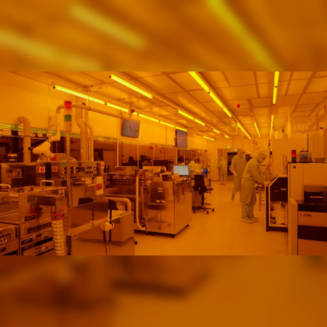
This is a hands-on role where you will work directly with wafers and photonic devices in our cleanroom. You will contribute to developing technologies that can be integrated into our photonics platform, working across multiple process steps rather than focusing on a single specialized process.
You will collaborate closely with experienced R&D engineers, scientists, and cross-functional teams. Depending on your experience, you will take ownership of individual technical activities and progressively grow towards leading larger development projects.
You will report to our Cluster Lead Engineering.
Your Responsibilities
Support the development of photonic integrated circuits and heterogeneous integration technologies from concept through processing, validation, and integration.
Perform hands-on wafer processing and chip fabrication in our cleanroom facility at the High-Tech Campus Eindhoven.
Execute and optimize semiconductor processing steps, including Etching, Metal deposition, PECVD and related thin-film processes and Other fabrication and process-development steps relevant to photonic devices
Develop and improve processing technologies that can be integrated into the SMART Photonics platform.
Work with different process modules and understand their interaction within the overall fabrication flow.
Contribute to process development, experimental planning, data analysis, and technical problem solving.
Support device development teams by translating technical requirements into practical processing solutions.
Perform experiments and support validation of new processes and technologies.
Analyze results, identify improvement opportunities, and contribute to the continuous improvement of our fabrication processes.
Contribute to technical reports, publications, patents, and EU project deliverables.
Collaborate with internal R&D teams and external partners, including universities, research institutes, and industry partners.
Gradually take ownership of technical work and, as you get more experience, lead larger development activities and projects.
Job requirements
We are looking for an enthusiastic R&D engineer who enjoys hands-on development, learns quickly, and is motivated to work across different aspects of photonic processing.
For this role, you will need:
At least a master’s degree in Photonics, Electrical Engineering, Physics, Materials Science, Chemical Engineering, or a closely related field.
Hands-on experience with semiconductor wafer processing and/or cleanroom fabrication.
Practical experience with processing steps such as etching, metal deposition, PECVD, or other semiconductor fabrication technologies.
Experience with III-V semiconductor materials such as InP, GaAs, or related compound semiconductors is highly preferred.
A broad interest in semiconductor and photonic processing.
Strong analytical and problem-solving skill.
Good communication skills and the ability to work effectively with colleagues from different technical disciplines.
A growth mindset: you are eager to learn, adapt to new challenges, share knowledge, and develop your expertise.
A proactive and collaborative attitude, with the ability to work effectively in a dynamic and evolving R&D environment.
A willingness to take responsibility and progressively develop towards greater technical and project ownership.
What we offer
A challenging position with the opportunity to make a tangible contribution to the development of next-generation photonic technologies.
A talented and passionate international R&D team with a diverse mix of nationalities, backgrounds, and expertise.
An open and collaborative culture where you are encouraged to adapt, share knowledge, take ownership, and grow.
Personalized career development through training, coaching, and technical development opportunities.
Access to specialised training, including JePPIX courses, Design for Six Sigma (DfSS), Green/Black Belt and Six Sigma training, and Project Management.
Unique workplace benefits, including chair massages, fresh fruit, fitness discounts, and Lunch Walks.
How we create a safe work environment together.
Security is a shared responsibility. At SMART Photonics, we are committed to providing a safe, inclusive, and respectful workplace, where everyone is treated fairly. Together, we protect our people, information, technology, and operations. Every employee is expected to work responsibly by following approved procedures, using our systems and information with care, and speak up when something doesn't seem right. By applying, you agree to uphold our security principles and Code of Conduct.
or
All done!
Your application has been successfully submitted!
You've already applied for this job
We appreciate your interest in this position. Unfortunately, you have already applied for this job.