Senior Scientist - Heterogenous Integration
- On-site
- Eindhoven, Noord-Brabant, Netherlands
- Technical Competence Centre TCC
Collaborative Environment and Strategic Impact: Play a key role in shaping the future of integrated photonics, influencing product strategies, and participating in high-impact EU projects.
Job description
We are seeking an experienced R&D Scientist with a strong industrial background in integrated photonics and Heterogeneous Integration. The ideal candidate will have hands-on expertise in developing and optimizing photonic components and in particular Micro transfer printing for the integration of InP SOAs, lasers, PDs and modulators on both SOI and SIN PICs . This role is particularly suited for professionals who have worked in the Hybrid/Heterogeneous Integration field and can apply their knowledge directly to product development and innovation.
An important element in this role is the support towards related EU projects by communicating with our partners and the outside world and contributing to the definition of our product strategy.
Key Responsibilities:
Be the technical lead of a cross functional development team, taking into account design, process and electrical/optical performance considerations.
Take a key role in technical discussions with external partners and customers, from early engagement stage. Take part in the technical assessment of new projects.
Advise the leadership team on the direction of the developments and give input to the technology roadmap
Lead and guide the technical team, focus on planning, execution, analysis, and based on that, recommendations for the next step, in a methodological way of working.
Assess the impact of process variables on device performance
Understand the interactions between different technical modules, while developing robust and reproducible technology platform.
Collaborate with cross functional teams as well as consortium partners (development institutions, wafer foundries, equipment manufacturers) and internal teams to ensure project objectives are met.
Job requirements
Qualifications:
Master's or PhD in Photonics, Electrical Engineering, Physics, or a related field.
10+ years of experience in III/V Semiconductor manufacturing processes.
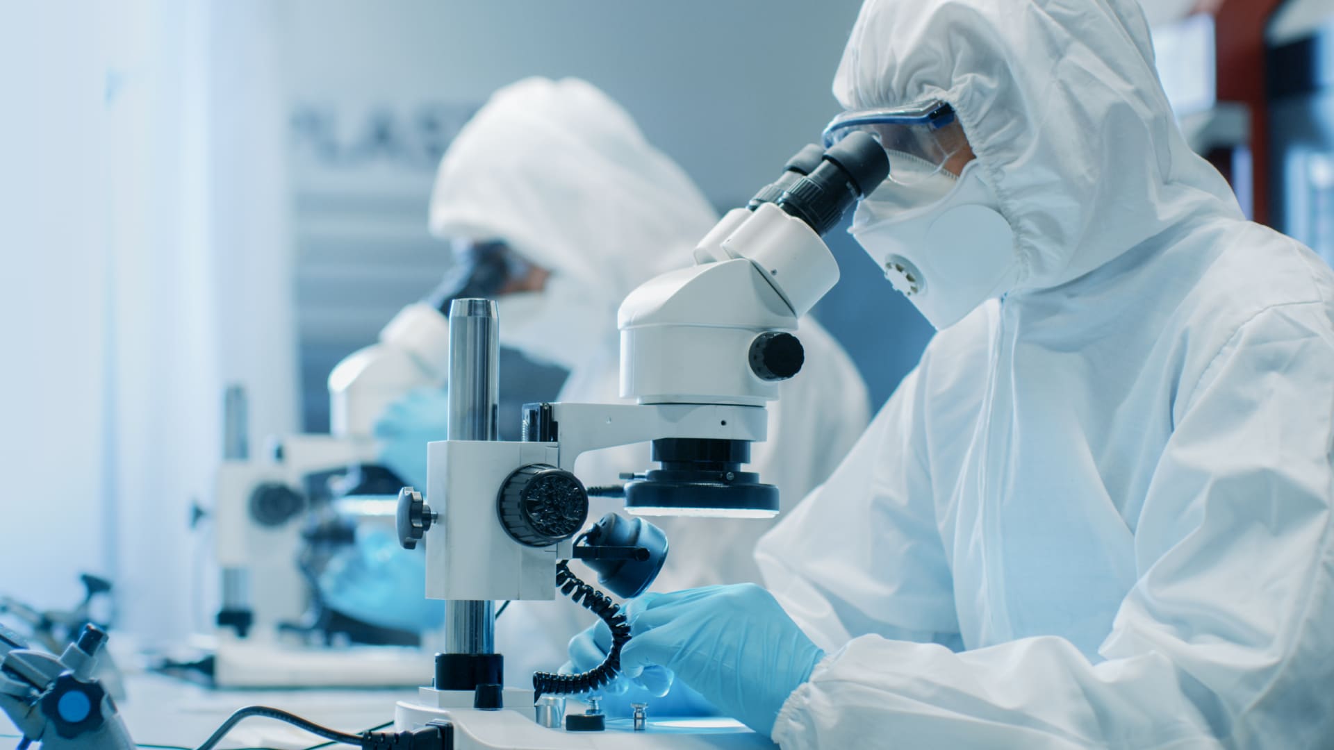
Hands on experience in working in a clean room environment.
Minimum of 4 years of hands-on industrial experience in integrated photonics, preferably in Micro Transfer Printing.
Familiarity with InP photonic platforms and integration techniques.
IDEAL CANDIDATE:
Strong project ownership mindset with a proactive, solution-oriented approach to industrial R&D challenges.
Excellent communication skills with cross-functional collaboration experience
Demonstrated success in networking in the SiPho/Micro transfer printing community (wafer foundry, post processing, equipment design and manufacturing) and maintaining strategic connections
Proven track record in Micro-transfer printing Experience in coordinating and reporting on EU projects.
Knowledge of Photonics and Indium Phosphide (InP).
Experience in optical and electrical characterization of photonic devices
Ambitious, self-oriented, and open to occasional travel
Proficient in English;
or
All done!
Your application has been successfully submitted!