Device Integration Engineer
- On-site
- Eindhoven, Noord-Brabant, Netherlands
- integration engineering
We are growing rapidly and are on the lookout for passionate individuals ready to shape the future of technology.
Job description
Team Mission
The Product Integration Engineering team is dedicated to maturing our core technology platforms and refining our Process Design Kit (PDK) so that customers can successfully build their photonics integrated circuits (PICs) with us. We are committed to refining our technology and enhancing our methodologies to enable rapid, efficient adaptations in our manufacturing landscape. This approach ensures we can swiftly turn customer designs into manufactured realities without sacrificing quality.
Role Summary
As a Device Integration Engineer, you will work at the intersection of design, process development, and Test&Measurement to improve the performance and manufacturability of our photonic platforms. You will play a vital role in correlating test device data with yield and process performance metrics, refining our PDK, and enabling successful product integration for our customers.
Key Responsibilities
Integrate design, process, and test deliverables to ensure customer designs are manufacturable, scalable, and meet performance expectations.
Analyze and correlate test data from devices and circuits to process performance (end-of-line data to in-line data) to identify improvement areas in both yield and platform performance. Create and maintain relevant dashboards and scripts.
Drive cross-functional improvement projects based on the analysed data which will enhance PDK capabilities, design rules, and overall platform robustness. Act as a driving force to link various teams.
Integrate simulation results with measured performance to refine PDK models.
Collaborate closely with yield and process engineers to define and execute yield ramp-up plans.
Guide test engineers in defining and executing appropriate measurement strategies and test structures.
Interface with Mask Design and PDK teams to ensure high-quality tape-outs and efficient design cycles. Ensure customer designs are manufacturable and scalable.
Support customer-facing technical discussions, as well as structured problem-solving (e.g. 8D) for issues related to yield or performance.
Job requirements
PhD in Photonics (preferred) or related field; Candidates with a MSc degree in Photonics or related field and 3 years of hands-on experience in integrated InP photonics or Si/SiN/LiNbO₃/hybrid photonics on top are also encouraged to apply.
Strong background in photonic device design, characterization, and data analysis (Python, MATLAB, Spotfire, etc.).
Extensive practical experience with data visualization/analysis tools as well as statistical process control (SPC) and design of experiments (DOE) and their analysis (JMP, Minitab, etc.) is a strong plus.
Understanding of PDK development, compact modelling, design rules, and circuit simulations. Hand on experience with tapeouts is a big plus.
Effective communication, stakeholder coordination, and a results-driven, pragmatic mindset.
Ability to work in cross-functional teams and translate technical insights into design and process improvements.
What we offer
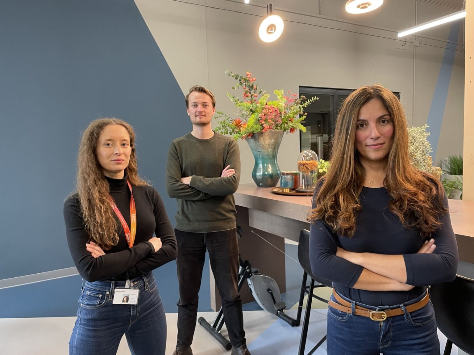
Be part of a collaborative, multicultural team, who is working at the forefront of Photonics innovation;
Work on exciting projects that are challenging and fun.
A tailored career development with training and coaching for growth
Work at the High Tech Campus, the SMARTest square kilometer in Europe!
or
All done!
Your application has been successfully submitted!